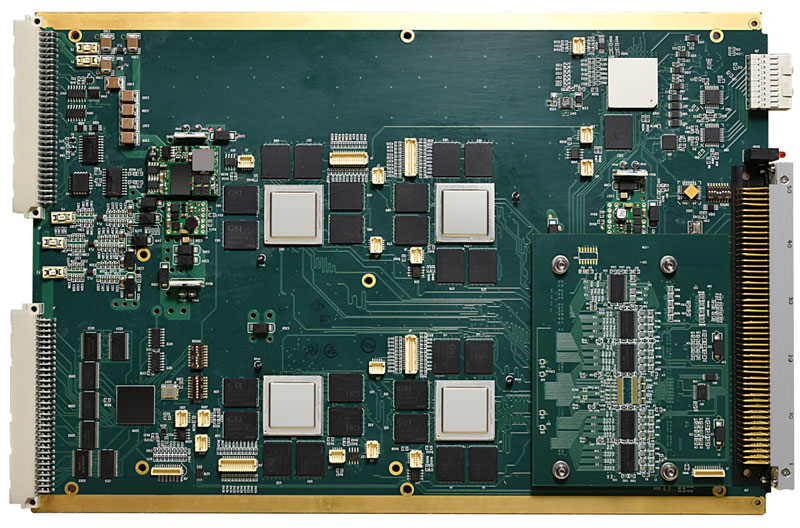
50 MHz Digital Word Generator (DWG)
A 50 MHz Digital Word Generator (DWG) that is a digital subsystem that executes diagnostic and/or functional test sequences in a standard VXI chassis. It is a suitable replacement for obsolete HP/Agilent 75000 Series C, Model D20 Digital Functional Test System, HP/Agilent E1450A Timing Modules, E1451A Pattern I/O Modules, E1452A Terminating Pattern I/O Modules, E1453A Timing Pods, E1454A Pattern I/O Pods, E1455A Timing Pods, and E1456A Pattern I/O Pods. It is also a 20 MHz Digital replacement, and an Interface Technologies replacement. Supports LASAR TAP files.
- Superior LRU/WRA Support
- 64 Bidirectional Channels Per Card
- 1 Megabit of Memory Per Channel
- Serial or Parallel Mode
- Master/Slave Timing Per Card in Chassis
- Cards Run Independent or Synchronized
- Trigger/Controls & Qualifiers Per Card
- Graphic Vector & Timing Editor
- Discrete Levels to Specification as Required
Characteristics and Specifications:
Pattern Rate
| Rate |
727 uHz - 50 MHz |
| Placement Resolution |
10.0 pS |
| Pin Skew |
< 3 nS Typical |
Sequencer Specifications
| Memory Depth Per Pin |
1 Mega-Vectors |
| Independent Memories: |
|
| PAT MEM/RAMs: |
|
| 8 Response |
1 Mega-Patterns |
| 8 Stimulus |
1 Mega-Patterns |
| 8 Reference |
1 Mega-Patterns |
| Timing: |
|
| Seq RAM |
1 Mega-Vector |
| Timing Cycle RAM |
32 bits x 16 K |
| Continuous/Loop Pattern |
Yes |
| Real-time Compare |
Yes |
| Stop on Error |
Yes |
| Stop on Error Bit |
Yes |
| Breakpoints |
Yes |
| Output Markers |
Yes |
| Trigger |
Yes |
| Conditions |
Yes |
Timebase Specifications
| Minimum Timing Cycle Duration |
20 nS or 4 Subcycle |
| Maximum Timing Cycle Duration |
16K Timing Cycles |
| Timing Cycle Resolution |
1 Subcycle |
| Minimum Timing SubCycle Period |
5 nS / 6.25 nS |
| Maximum Timing SubCycle Period |
83.8 mS |
| SubCycle Period Resolution |
5 nS / 6.25 nS |
| SubCycle Period Accuracy |
1 PPM |
Control Timing/Pod Specifications
| Minimum Edge Timing Delay |
0 Subcycles |
| Maximum Edge Timing Delay |
Timing Cycle Duration - 1 Subcycle |
| Edge Timing Resolution |
1 Subcycle |
| Minimum Programmable Pulse Width |
10.0 nS |
| RiseTime |
<5 nS, typical |
| FallTime |
<5 nS, typical |
| Sustained Output Current |
+/- 24 mA |
| Logic High, Open Circuit |
5 V, minimum |
| Logic High, Sourcing 24mA |
2.5 V, minimum |
| Logic Low, Open Circuit |
0.1 V, maximum |
| Logic Low, Sinking 24mA |
0.44 V, maximum |
Triggers and Timing Port Specifications
| Input Sources |
8 VXI TTL Buses, 2 VXI ECL Buses, 2 Front Panel |
| Slopes |
Programmable |
| Qualifiers |
Boolean expression, up to 10 'Q' inputs, 1 end if ready |
| 'Q' Input High |
>2.0 V (internal pull-up) |
| 'Q' Input Low |
< 0.8 V at < 150 uA |
| 'Q' Input Capacitance |
<10 pF |
| 'Q' Inputs Latency |
70 nS Typical |
| Front-panel TTL High |
>2.0 V (internal 50 K pull-up) |
| Front-panel TTL Low |
< 0.8 V at < 25.0 mA |
| Front-panel TTL Capacitance |
<10 pF |
| Minimum TTL Trigger Pulse Width |
6 nS |
| Minimum ECL Trigger Pulse Width |
no ECL front panel |
| Minimum Time Between Triggers |
10.0 nS + Programmed Trigger Delay |
| Programmable Delay |
0 to 327.68 uS in 5 nS steps or 0 to 409.59375 uS in 6.25 nS steps |
| Output Marker |
Anywhere |
Output Port Specifications*
| Sustained Output Current |
+/- 24 mA |
| Logic High, Open Circuit |
5 V, minimum |
| Logic High, Sourcing 24mA |
2.5 V, minimum |
| Logic Low, Open Circuit |
0.1 V, maximum |
| Logic Low, Sinking 24mA |
0.44 V, maximum |
| Capacitance (disabled) |
30 pF, maximum |
| Leakage Current (disabled) |
120 uA, maximum |
| RiseTime |
>6.5 nS |
| FallTime |
>7.0 nS |
| Tri-state Input Delay |
8 nS, typical |
Input Port Specifications*
| Logic Low |
<0.8 V at <150uA |
| Logic High |
>2.0 V (internal pull up) |
| Real-Time Compare Mask |
Static don't care pins |
| Real-Time Compare Control |
Vector by Vector enabling |
| Sample format |
Edge |
|
|
*Custom levels by specification only